In the world of material science, what you see on the surface is only part of the story. The true performance, durability, and reliability of a material are dictated by its internal architecture and chemical makeup. For laboratory professionals, understanding this hidden world is not just a curiosity—it’s a necessity. Microstructural analysis and compositional analysis are the two foundational pillars of this investigation, providing the deep insights needed to solve complex problems, ensure quality, and drive innovation.
From the fine-grained structure of a high-performance alloy to the elemental composition of glass used in fiber optics, these analytical techniques provide a critical window into how and why a material behaves the way it does. They are essential for everything from quality control and product development to forensic-style defect analysis and research. This article explores these vital disciplines, the powerful tools that make them possible, and their profound impact across various industries.
The Fundamentals of Microstructural Analysis
Microstructural analysis is the study of the structure of a material, typically on a scale from the nanometer to the centimeter. This includes the size, shape, and arrangement of grains, phases, precipitates, and defects. The microstructure directly influences a material’s properties, such as its strength, toughness, hardness, and corrosion resistance. By manipulating the microstructure through processing, engineers can fine-tune a material’s performance to meet specific application requirements.
For example, in the production of ceramics, the grain size distribution is a crucial factor. Smaller grains can often lead to higher strength and toughness, while larger grains can be associated with certain mechanical or thermal properties. A material that is improperly heat-treated or sintered can develop an undesirable microstructure, leading to premature failure.
Key aspects of microstructural analysis include:
- Grain Size and Shape: The physical dimensions and morphology of individual crystal grains.
- Phase Distribution: The identification and spatial arrangement of different chemical phases within the material.
- Pore and Void Characterization: The size, shape, and distribution of pores, which can significantly affect material density and strength.
- Defect Detection: Identifying and characterizing imperfections like cracks, inclusions, or dislocations that can compromise material integrity.
This type of analysis is often performed using optical microscopy for larger-scale features, but it truly excels with advanced techniques like Scanning Electron Microscopy (SEM).
The Power of Compositional Analysis
While microstructure tells us about the physical arrangement of a material’s components, compositional analysis reveals its chemical identity. It answers the fundamental question: “What is this material made of?” This can be on a macro-scale (the overall elemental makeup) or a micro-scale (the composition of specific, localized features).
For manufacturers, ensuring the correct elemental recipe is followed is paramount. An incorrect alloy blend or an impurity in raw materials can lead to catastrophic product failure. Take, for instance, glass used in high-tech applications. Even minute amounts of certain impurities, such as iron oxides, can change the optical properties of the glass, making it unsuitable for its intended use.
Compositional analysis provides vital data for:
- Quality Control: Verifying that a material’s chemistry matches its specifications.
- Reverse Engineering: Determining the composition of a competitor’s product or an unknown sample.
- Forensic Analysis: Identifying contaminants or precipitates that caused a material to fail.
- Process Monitoring: Tracking changes in composition during manufacturing to ensure consistency.
Together, microstructural and compositional analysis provide a holistic view of a material, allowing scientists and engineers to fully understand its nature and predict its behavior.
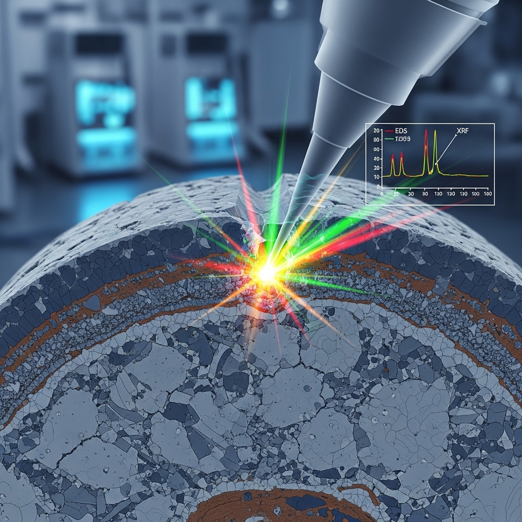
Key Techniques for SEM/EDS and XRF Analysis
The tools available for microstructural and compositional analysis have evolved significantly, offering unprecedented resolution and data quality. Among the most widely used and powerful techniques are Scanning Electron Microscopy with Energy-Dispersive X-ray Spectroscopy (SEM/EDS) and X-ray Fluorescence (XRF analysis).
Scanning Electron Microscopy (SEM): SEM uses a focused beam of electrons to scan the surface of a sample. As the electrons interact with the material, they produce various signals, which are then used to create a highly magnified, three-dimensional image of the sample’s surface. This allows for the detailed visualization of microstructure, including grain boundaries, surface texture, and defects, at resolutions far beyond what is possible with traditional optical microscopes. The ability to visualize the intricate details of ceramics, for example, has been a game-changer for materials research and quality assurance.
Energy-Dispersive X-ray Spectroscopy (EDS): EDS is a powerful compositional analysis tool that is almost always coupled with an SEM. When the electron beam from the SEM hits the sample, it can knock electrons out of the atoms within the material. To fill these vacancies, electrons from higher energy levels drop down, emitting X-rays with energies characteristic of that specific element. The EDS detector measures the energy and quantity of these X-rays, providing a highly localized elemental analysis of the sample. This allows an analyst to not only see a defect with the SEM but also determine its precise chemical composition.
X-ray Fluorescence (XRF): XRF is another form of elemental analysis, but it provides a bulk or surface-level compositional analysis, rather than the highly localized data of EDS. In XRF, a sample is bombarded with high-energy X-rays, causing the atoms to emit secondary (fluorescent) X-rays. Like with EDS, the energy of these X-rays is unique to each element, allowing for a qualitative and quantitative determination of the elements present. XRF is a non-destructive technique and is highly effective for rapid screening and quality control, especially for samples like compositional analysis glass or metal alloys where a quick, overall chemical fingerprint is needed.
Comparison of Techniques:
| Technique | Primary Function | Spatial Resolution | Destructive? | Key Application |
|---|---|---|---|---|
| SEM | Microstructural Imaging | High (nanometer scale) | No | Defect analysis, surface morphology |
| EDS | Elemental Analysis | High (micron scale) | No | Localized composition of phases |
| XRF | Elemental Analysis | Lower (bulk or surface) | No | Rapid elemental screening, QA/QC |
These techniques, often used in combination, provide a comprehensive suite of tools for material characterization.
Integrated Approach: From Defect Analysis to Material Characterization
In a real-world scenario, these techniques are rarely used in isolation. A typical workflow for material characterization or defect analysis might look something like this:
- Initial Observation: A failed part or a non-conforming sample is received. Initial inspection using optical microscopy reveals a surface crack.
- Microstructural Investigation (SEM): The sample is prepared for SEM. High-resolution imaging confirms the presence of a fracture and reveals the fracture’s morphology (e.g., brittle vs. ductile). Further SEM analysis may show the presence of a foreign inclusion or an unusual grain structure at the origin of the crack.
- Compositional Confirmation (EDS): Using the EDS detector on the SEM, the analyst performs a point analysis on the foreign inclusion identified in the SEM image. The EDS spectrum reveals that the inclusion is a silica-rich particle, which should not be present in the material.
- Overall Composition (XRF): A quick XRF scan of the material’s surface confirms that the overall bulk chemistry of the part meets the original specifications, confirming that the failure was not due to an incorrect alloy blend but rather a localized contamination.
This combined approach allows for a precise diagnosis of the failure mechanism and provides actionable data to prevent future issues. It is this synergy between visualizing the structure and identifying the composition that makes these analyses so powerful and indispensable for any laboratory focused on material integrity. The ability to perform this kind of detailed analysis on challenging materials like ceramics is what separates a good lab from a great one.
Unlocking Innovation: The Strategic Value of Material Characterization
Microstructural and compositional analysis are not just academic exercises; they are essential for maintaining quality, ensuring safety, and accelerating innovation. By leveraging advanced techniques like SEM/EDS and XRF, laboratories can gain an unparalleled understanding of the materials they work with. This knowledge translates directly into improved product performance, reduced costs from material failure, and a stronger competitive edge. It is the definitive path to true material characterization.
Submit a testing request today to find a lab that specializes in microstructural and compositional analysis to solve your toughest material challenges.
Frequently Asked Questions
SEM provides high-resolution images of a material’s surface, revealing its microstructure and morphology. While often paired with EDS for localized elemental analysis, XRF is a separate technique that provides a bulk or surface-level elemental composition without imaging.
Defect analysis identifies the root cause of a material failure or a quality issue. By understanding why a product failed (e.g., a foreign inclusion, improper heat treatment, or a material flaw), businesses can implement corrective actions in their manufacturing processes to prevent future costly failures.
Yes, absolutely. Techniques like EDS and XRF are widely used for the compositional analysis glass, polymers, ceramics, and other non-metallic materials. They are versatile tools for determining the elemental makeup of almost any solid sample.
While microstructural analysis ceramics is a key application, these techniques are used across a vast range of materials, including metals, polymers, composites, and semiconductors. The principles remain the same: understanding how the internal structure of a material influences its properties.
This content includes text that has been generated with the assistance of AI. Contract Laboratory encourages the use of new tools and technologies that enhance our editorial process. Our full editorial policy can be found here.